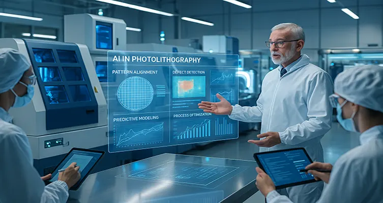
Photolithography is the heart of semiconductor manufacturing, responsible for etching intricate circuit patterns onto silicon wafers with nanometer precision. As chip architectures grow increasingly complex, the margin for error in this process has become razor-thin. Even the slightest misalignment or distortion can compromise entire batches of wafers, driving up costs and slowing production. Artificial intelligence is emerging as a powerful tool to address these challenges, predicting exposure outcomes and enabling finer control over every stage of lithography. Erik Hosler, a semiconductor innovation expert, underscores that AI’s precision-driven role in manufacturing is unlocking levels of accuracy once thought impossible. His perspective reflects the growing realization that the future of photolithography lies in data-driven intelligence.
This development arrives at a crucial moment. With demand for smaller, faster, and more energy-efficient chips at an all-time high, manufacturers must push lithography equipment beyond traditional limits. Extreme Ultraviolet (EUV) lithography, for example, operates at the forefront of what physics allows, where even minor deviations can result in critical defects. AI-enhanced control systems give fabs the ability to anticipate variations, compensate for them in real time, and achieve higher yields. By turning lithography into a predictive and adaptive process, AI is reshaping one of the most delicate stages of chip production.
The Critical Role of Photolithography
Photolithography determines how precisely transistors and interconnects are patterned, directly influencing chip density, performance, and power consumption. Historically, advances in lithography, shrinking wavelengths of light and refining optics have been central to keeping pace with Moore’s Law.
However, as dimensions approach atomic scales, traditional methods face fundamental limitations. Factors such as light diffraction, lens imperfections, and material variability introduce distortions that no amount of hardware alone can fully correct. As a result, engineers increasingly rely on computational techniques to improve accuracy. Yet even with these improvements, predicting and controlling exposure outcomes at advanced nodes requires capabilities that exceed human intuition and conventional algorithms.
AI as a Predictive Engine
AI changes the equation by acting as a predictive engine that learns from massive datasets of lithography outcomes. Machine learning models can analyze thousands of historical wafer images, process variables, and equipment parameters to predict how specific settings will influence exposure accuracy. Instead of relying solely on trial and error, fabs can now simulate and refine results before wafers ever reach the production line.
This predictive capability is particularly valuable for EUV lithography, where equipment costs are incredibly high and throughput must be maximized. By anticipating variations in exposure, AI models help optimize parameters such as dose, focus, and mask alignment. The result is greater consistency across wafers, improved yield, and reduced production costs.
Improving Precision Through Adaptive Control
Beyond prediction, AI also drives adaptive control during the lithography process itself. As wafers are exposed, real-time data from sensors can be fed into AI models that detect deviations and adjust parameters immediately. This closed-loop system ensures that even when conditions shift slightly due to equipment wear, environmental changes, or material inconsistencies, the process remains stable.
Such adaptive control is vital because variations that seem microscopic can have large-scale consequences. By maintaining precision dynamically, AI allows fabs to produce circuits with higher fidelity to design specifications. This capability extends the life of existing lithography equipment while ensuring it can keep up with next-generation chip designs.
Precision at the Sub-Nanometer Scale
The move to sub-nanometer control is where AI truly demonstrates its value. Traditional inspection methods often fall short when trying to identify the tiniest distortions or overlay errors. By combining high-resolution imaging with machine learning analysis, AI provides insights at scales previously unattainable. Erik Hosler emphasizes, “Free-electron lasers are revolutionizing defect detection by offering unprecedented accuracy at the sub-nanometer scale.”
His point highlights how AI-integrated technologies can achieve a level of precision that fundamentally reshapes lithography control. What makes this advancement transformative is not only the detection of errors but also the ability to prevent them. With predictive and adaptive tools, fabs can minimize defects before they compromise yield, saving both time and resources in an industry where every wafer counts. These improvements translate directly into competitive advantage.
Industry Benefits of AI in Photolithography
The integration of AI into lithography is producing ripple effects across multiple sectors. In consumer electronics, improved lithography precision allows for denser chips that power faster, more efficient smartphones and laptops. In the automotive industry, where chips must balance reliability with performance, AI-enhanced control ensures that processors meet rigorous safety standards.
Data centers and AI infrastructure also benefit from the gains in yield and efficiency. As demand for high-performance processors continues to grow, the ability to produce more reliable chips at scale helps meet global needs while containing costs. Looking forward, these improvements also pave the way for breakthroughs in advanced packaging and 3D integration, which depend on perfect alignment between layers of circuitry.
Overcoming Barriers to Adoption
Despite its promise, integrating AI into photolithography control systems presents challenges. The volume of data required to train accurate models is immense, and managing this information requires advanced infrastructure. Additionally, legacy lithography equipment may need retrofitting to support AI-driven control, creating significant upfront costs.
There is also the issue of trust and interpretability. Engineers must be confident in AI recommendations, particularly when dealing with high-stakes, high-cost equipment like EUV scanners. Developing transparent AI systems that can explain their outputs will be essential for ensuring widespread adoption.
Redefining the Limits of Lithography
AI is pushing photolithography into a new era of predictive and adaptive precision. By forecasting outcomes, adjusting parameters in real time, and enabling control at the sub-nanometer level, AI is transforming one of the most challenging aspects of semiconductor manufacturing. The technology does more than correct errors because it helps prevent them altogether, setting the stage for higher yields and more efficient production.
As demand for advanced chips accelerates, fabs that embrace AI-driven photolithography will hold a distinct edge. These innovations are not just incremental improvements. They are redefining what is possible in semiconductor design and manufacturing. In the process, AI ensures that progress continues, even as the physical limits of light itself are tested.